
As LED display technology continues to evolve, fine-pitch LED screens have gradually become the market mainstream. However, as pixel pitches shrink and viewing distances decrease, the “Yin-Yang screen” issue—where brightness appears uneven across the display—has become increasingly prominent. What exactly is this issue, how does it arise, and what effective technical solutions exist? Let us delve into this topic to provide technical insights for improving LED display quality and performance.
LED displays are created by mounting LED components in an array on a PCB surface. In the era of coarse-pitch LED screens, visual discrepancies caused by insufficient mounting precision were rarely noticeable due to longer viewing distances and the presence of protective masks. In recent years, however, as pixel pitches have narrowed and viewing distances have shortened, the precision requirements for LEDs, PCBs, and the mounting process have become extremely stringent. Consequently, even minute manufacturing defects—such as a slight tilt in the light-emitting surface—become apparent at close range, making the Yin-Yang screen issue highly visible.
The Yin-Yang screen issue refers to a phenomenon where the display appears noticeably dimmer or brighter when viewed from the left side, while the opposite effect (brighter or dimmer) occurs when viewed from the right, creating a distinct contrast in brightness between the two viewing angles.
The root causes of the Yin-Yang screen issue lie primarily in three areas: the LED components (beads), the PCB, and the mounting process.
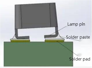
Consider the selection of LED components. In fine-pitch LED screens, CHIP-type and TOP-type LEDs are common examples. CHIP-type LEDs utilize BT-material substrates for die bonding and wire bonding, whereas TOP-type LEDs connect to the PCB via bent copper leads. With TOP-type LEDs, if the lead bending angle approaches 90 degrees, uneven solder paste distribution on the PCB can cause the LED to tilt. Therefore, when selecting TOP-type LEDs, engineers typically avoid components with right-angle bends in favor of those with “hook-shaped” leads. The advantage of the “hook-shaped” terminal design is that it eliminates the need for precise solder paste volume control; during reflow soldering, excess solder can flow into the adjacent spare space, ensuring the LED package sits flush against the PCB. Furthermore, strict control over terminal coplanarity and dimensional tolerances ensures the LED remains level after placement, thereby enhancing display quality.
Next is the control of the SMT (Surface Mount Technology) process. During LED placement, stencil printing and reflow oven temperature control are critical factors in preventing “light/dark screen” issues (uneven brightness or color). For fine-pitch LED displays, individual terminal dimensions range from 0.2×0.2mm to 0.5×0.5mm; the relatively small stencil apertures make them prone to clogging. Applying new coating materials can reduce solder paste stringing, and regular stencil cleaning is essential. Reflow profiles also affect solder melting; monitoring these profiles during every production shift ensures product stability. Additionally, since LEDs are directional components, consistent orientation must be verified before they enter the reflow oven.
Finally, there is the PCB factor. The manufacturing precision of the pads on the display side of the PCB directly impacts placement accuracy and is a key factor in preventing brightness/color uniformity issues. If the pad size is smaller than the solder mask opening during PCB design, the pad may shift away from the center of the opening. Since the area surrounding the pad within the opening is usually coated with solder mask ink—which is often thicker than the pad itself—ink accumulation can occur, obstructing solder flow and causing uneven distribution, which leads to LED tilting. This issue can be resolved by optimizing the dimensional relationship between the pads and the solder mask openings and by tightening quality control during PCB manufacturing.
In summary, effectively addressing LED component selection, SMT process control, and PCB precision management can successfully prevent brightness/color uniformity issues in LED displays. As technology advances, we are confident that these issues will be better resolved in future LED display manufacturing, delivering superior visual experiences to users.